By Sue Mohieldin | May 27, 2021
Introduction
Welcome back to our introduction to hardware hacking 101 series and our second installment of our JTAG blog post! In this post we share a teardown of a TP-Link AC1750 to demonstrate how to identify and verify a pinout for JTAG. If you haven’t already, make sure to check out part one of the JTAG post where we provide background on the interface and its characteristics.
Hands On
Now that we have covered how JTAG works and its interface, let’s take a look at a TP-Link Archer C7 | AC1750 dual band wireless router to demonstrate how to locate and identify the pinout for JTAG.
TP-Link AC1750 Tear Down
The first step to locating JTAG is disassembling the device and gaining access to the PCB.
Remove the 4 screws located at the bottom of the device and then lever the device open by separating the top and bottom casing.
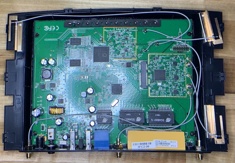
Carefully remove the antennas from the PCB if desired to have unrestricted access to the top and bottom of the PCB.
Chip and Header Identification
Now that we have full access to the board, we will identify the main chips and any headers or test points that can be suitable JTAG candidates.
Chip ID Table
| Location | Manufacturer | Model | Description | Chip Image |
|---|---|---|---|---|
| U1 | Qualcomm | QCA9558-AT4A | Integrated SoC for AP routers/ MIPS processor | 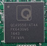
|
| U1 on daughtercard at J6 | Qualcomm | QCA9880-BR4A | Integrated SoC for AP routers/ processor | 
|
| U8 | Atheros | AR8327 | Gigabit ethernet switch | 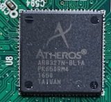
|
| U11 & U26 | Winbond | W9751G6KB | 512M bits DDR2 SDRAM | 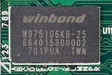
|
| U6 | Winbond | 25Q128FVSG | SPI flash | 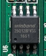
|
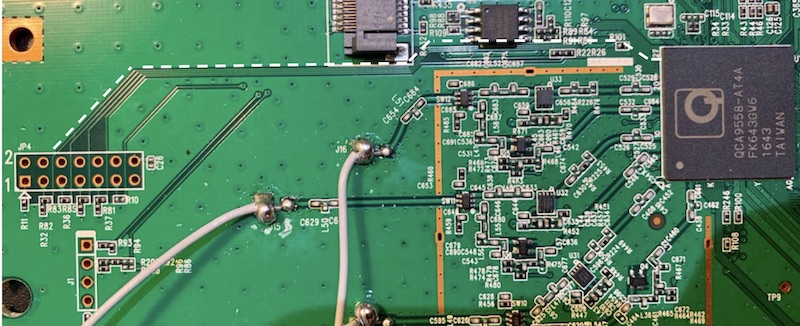
Removing the daughter PCB connected via J6, we see that there are a few traces that run to QCA9558-AT4A, making it a likely candidate for JTAG or another debug interface for this SoC. The following figure highlights the traces in white.
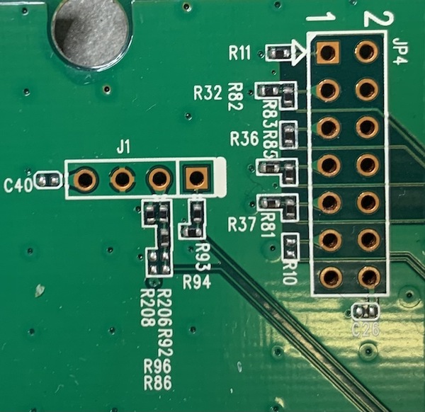
The next step is to start identifying some of the pins. The easiest pins to identify are GND, which can be verified by performing continuity tests using a multimeter. Also using a multimeter, we will measure the impedances of the pins to GND and Vcc when the device is powered off and on, and also measure the voltages of the pins.
2x7 Header Electrical Characteristics Table
The following table identifies the electrical characteristics of the 14 pins. Note that the GND pins were identified by continuity testing and the impedances were filled out for added detail.
| Pin | RGND (Ω) | RVcc (Ω) | Voltage (V) | Notes | Pin | RGND (Ω) | RVcc (Ω) | Voltage (V) | Notes |
|---|---|---|---|---|---|---|---|---|---|
| 1 | 9.96k | 10.18k | 0 | TBD | 2 | 0 | 222 | 0 | GND |
| 3 | 6.91k | 7.24k | 0 | TBD | 4 | 0 | 222 | 0 | GND |
| 5 | 0.346M | 0.344M | 10m | Maybe TDO? | 6 | 0 | 222 | 0 | GND |
| 7 | 6.94k | 7.23k | 0 | TBD | 8 | 0 | 222 | 0 | GND |
| 9 | 6.94k | 7.23k | 0 | TBD | 10 | 0 | 222 | 0 | GND |
| 11 | inf | inf | 2.4m | TBD | 12 | inf | inf | 6.2m | TBD |
| 13 | inf | inf | 1.1m | TBD | 14 | 5.99k | 6.13k | 2.61 | Most likely vref (a bit lower than 3.3V hence why there is some resistance against 3.3V) |
Note: The table is formatted to match the pin layout on the PCB
So far using our multimeter, we were able to locate 5 GND pins, a likely VREF pin connector which appears to be operating at a slightly lower voltage of 2.61V and a potential TDO pin, which has high impedance. The next task is to try and find a standard header. Since we are confident that we have correctly located the GND pins, it is easiest to try and match our GND pin orientations. Ideally, the pinout would also match our likely VREF and TDO candidates. Furthermore, given that there are traces to the QCA9558-AT4A, which is a MIPS-based processor, our best bet would be to find the pinout for a MIPS 14-pin JTAG interface.
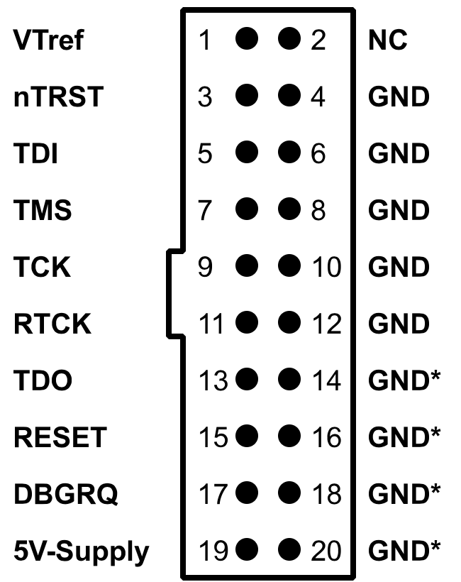
Luckily, the MIPS EJTAG 14 pin connector matches our GND pin orientations and the labeled VIO pin follows our theory that pin 14 is VREF as well as the suspected TDO pin. EJTAG stands for extended JTAG and is a MIPS extension of JTAG, allowing for reprogramming and debugging of MIPS processors. In this MIPS EJTAG connector, we see the 5 primary signals: TCK, TMS, TDO, TDI and TRST (test reset input). In addition, there is a RST pin which is the system reset, DINT, debug interrupt and VIO which is the voltage reference. The electrical EJTAG connection is shown in figure X.
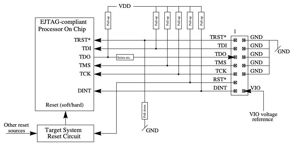
Electrical 14-pin EJTAG Connection. Source: MIPS Technologies Inc.
Testing the JTAG Pinout
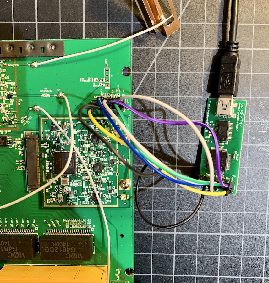
To test whether this pinout hypothesis is correct, we will connect TCK, TMS, TDI, TDO, TRST, VREF and GND pins to a GoodFET42, which is a multi-purpose debug tool and JTAG adapter to see whether a device is identified. We will also separately connect to a Segger J-Link, which is a more full-featured JTAG debugger to demonstrate another method of verifying the correct pinout.
Connecting to the GoodFET
For an easy connection, we solder a 0.1” PCB mount header. Next, we will connect TCK, TMS, TDI, TDO, TRST, VREF and GND to the GoodFET, as shown in the following figure. With the TP-Link powered on and in a stable steady state, we will test a couple of commands to validate whether our pinout hypothesis is correct.
$ ./goodfet.jtag detect
Initializing JTAG...OK
Detecting chain length...OK
  Chain length: 1
Getting ID for device 0...OK
  Device 0 ID: 0x00000001
$ ./goodfet.jtag chain
Initializing JTAG...OK
Detecting chain length...OK
  Chain length: 1
As shown, the GoodFET identified a chain length of 1 and a device ID.
Connecting to J-Link
To connect to the J-Link, we connect TCK, TMS, TDI, TDO, TRST, VREF and GND from the TP-Link to that of the J-Link. The following figure shows the pinout on the J-Link device.
J-Link Pinout. Source: SEGGER
Next, we open the JLinkExe, which gives us a command line to interact with the J-Link and test the target system. As shown, VTref is identified as 2.605V, which is the same value that we measured using the multimeter.
Connecting to J-Link via USB...O.K.
Firmware: J-Link V9 compiled Feb  2 2021 16:34:10
Hardware version: V9.30
S/N: 269302232
License(s): FlashBP, GDB
OEM: SEGGER-EDU
VTref=2.605V


Type "connect" to establish a target connection, '?' for help
J-Link>
Once connected, we can select a profile for the device/ core that we are trying to debug, which in this case is a MIPS core. To be more specific, the TP-Link has a Qualcomm and an Atheros chip on board and might therefore be a MIPS ath79 target. However, the J-Link only has MIPS PIC32 devices built in, as shown in the following figure.

Therefore, we had to build the configuration in OpenOCD (Open On-Chip Debugger), which we will discuss how to implement in a separate blog post. For now, let us look at the connection to the J-Link at a high a level and confirm whether we have the correct pinout and processor architecture.
In OpenOCD, we will open a debug session via telnet using the following command:
$  telnet localhost 4444
Trying 127.0.0.1...
Connected to localhost.
Escape character is '^]'.
Open On-Chip Debugger
Next, we will issue a reset and halt command to verify that the device is connected appropriately and test whether the chosen target architecture is correct.
> reset init
JTAG tap: ath79.cpu tap/device found: 0x00000001 (mfg: 0x000 (<invalid>), part: 0x0000, ver: 0x0)
timed out while waiting for target halted
TARGET: ath79.cpu - Not halted
Halt timed out, wake up GDB.
> halt
MIPS32 with MIPS16 support implemented
target halted in MIPS32 mode due to debug-request, pc: 0x80006380
As seen by our terminal output, we were able to successfully connect to the device. Furthermore, the same device 0x00000001 using the GoodFET was identified. Hence, our pinout hypothesis is likely correct, which will allow us to perform a lot more functions like reading and writing memory, changing the program counter, and more.
Conclusion
In this blog post we demonstrated how to locate JTAG on a target device and methodologically identify the pinout. The TP-Link device used as an example, conveniently had a 2x7 header exposed on the board, but this is not always the case. Sometimes, JTAG can be un-clustered test points across the board, making it more challenging to locate and identify. However, by identifying the chips on the board and knowing their functionality and processor architecture, it is possible to apply the same techniques and find JTAG in a consistent manner.
In our next post in the Hardware Hacking 101 series, we will cover how to communicate using JTAG once the pinout has been identified. The blog post will walk through OpenOCD and demonstrate how to read and write from memory. In the meantime, contact us at any time with questions or to discuss how we can help with your product security needs.